IXYS UK Westcode, part of the global power semiconductor manufacturer IXYS Corporation, is investing in its Chippenham factory to manufacture a new range of power semiconductor devices, which will be marketed alongside the company’s long-established Press-pack Capsules. X-ray equipment is needed to check the quality of the reflow soldering process during production.
Power semiconductor devices are designed for switching high currents and voltages; they are used widely in the rail, wind-turbine, mining and petrochemical sectors.
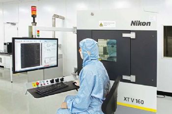
They combine integrated circuits and DCB (direct copper bonded) substrate technology. The company is using an XT V 160 X-ray system from Nikon Metrology (
www.nikonmetrology.com), because the reflowed solder (which attaches the chips to their contact pads) must be continuous and with a controlled level of voids; X-raying is the only way to see if these conditions have been met.
Fiona Lambert, process engineer at IXYS UK Westcode, said: “I previously used a smaller Nikon 130kV X-ray quality-assurance system when I worked at an electronics company in South Wales, so I knew how easy this equipment is to use.
"After reviewing what was available on the market, it was clear that Nikon’s more powerful 160kV model would best suit our application, which involves penetrating thicker and higher-density materials to observe solder coverage.
“What I particularly like about the Nikon system is the easy access to its large stage, which allows me to place several components on it at the same time.
"The machine is fast in operation, and the stage is easy to manipulate in multiple axes; this means that tilting, rotating and positioning — as well as zooming the image on the screen — is rapid.
"You can see everything clearly, as the image is high-resolution. Moreover, the software is user-friendly and even automatically works out the percentage of voids in the solder necessary to ensure that the product meets rigorous specifications.”
Two-stage inspection
X-raying is carried out at two stages of manufacture. The first is after the chips have been placed on the blank DCB substrate and reflow-soldered. After six built substrates have been electrically tested and soldered onto a 5mm-thick aluminium-silicon-carbide baseplate, the whole assembly is X-rayed again.
The XT V 160 inspects the assembly reliably, even without Nikon Metrology’s optional X-ray laminography software or CT (computed tomography) add-on.
Features of the machine that assist in completing the task efficiently include: a 20W target power rating; focal spot size between 1 and 10µm (depending on power output); up to 36,000-times system magnification; and the high image quality provided by a Varex ‘16-bit flat panel’.
Having such fine resolution allows easy distinction between geometrical shapes and the amorphous voids. Although the X-ray machine was installed specifically for DCB inspection, its presence on the Chippenham site has proved beneficial for verifying the quality of bought-in materials.
On one occasion, a supplier disputed that there was a high incidence of solder blockages in a consignment of delivered coolers that form part of Press-pack Capsules. A simple analysis using the XT V 160 provided irrefutable
evidence and resulted in the prompt delivery of a replacement batch.
An additional advantage of X-ray technology from Nikon Metrology is the stability of output due to the micro-focus spot source and advanced image-processing capabilities — essential to avoid degradation of image quality.
The focus of the electron beam is maintained by a computer-controlled electromagnetic lens, which ensures that the target does not overheat, while maintaining a ‘micron spot size’ — even at high kV settings.
Although it is a high-power machine, the XT V 160 is of open-tube design; and as part of planned maintenance, replacement of the electron-beam-producing filament can be scheduled a couple of times per year for a cost of a few pounds. Filament replacement takes minutes, so down-time is short.
On the other hand, a sealed tube will last for a couple of years but can stop working without warning — perhaps at the worst possible time for the user.
The manufacturer then has to be called in to renew the tube at a cost of many thousands of pounds, and the machine is down for days.
IXYS UK Westcode’s inspection of power semiconductor devices will increase over the coming years; and with one or two products per batch to be X-rayed for quality assurance, the Nikon Metrology machine will be in constant use, once the process has been finally established.
The transmission target X-ray source in this particular XT V 160 system was the 1,000th to be manufactured in the UK at Nikon Metrology’s Tring factory, where manufacturing began in 1987.