The semi-conductor market is booming. Microchips are not only essential for electric vehicles (EVs) and charging stations. They also play an important role in solar and wind power plants and the entire spectrum of communications technology. With expected growth rates of over 30% per year, this multi-billion dollar market offers interesting prospects for grinding technology.
At the
GrindingHub trade fair, organised by the
VDW (German Machine Tool Builders' Association) in Stuttgart from 5 to 8 May, visitors can gain insights into manufacturing, machines, and precision grinding processes in the angstrom range. One thing is certain — if Europe wants to catch up with Asia and the USA in the semiconductor industry, many things will have to happen faster, including in the production process.
Wafers are thin discs that serve as the basis for the manufacture of microchips. The wafers are manufactured in several processing steps. In order to use silicon (Si) or silicon carbide (SiC) in the semiconductor industry, it must be grown as a single crystal. The so-called ingots and boules are then processed into a blank puck. Sliced into pieces, the wafers are thinly ground, polished, and coated with an epitaxial layer to prepare them for the photolithography process. Circuit patterns are etched into the wafer using appropriate masks and light. Finally, individual microchips can be cut from the wafer.

For Michael Egeter (pictured left), vice president of engineering at Swiss machine manufacturer
Kellenberger in Goldach, the steady increase in demand from end customers and new processes and technologies ensure that involvement in the semiconductor market appears to be extremely worthwhile. He said: “In addition to the actual substrate processing — such as pre-grinding and cutting the raw crystals, creating the basic wafer geometry — the field of semi-conductor processing equipment also offers good opportunities to provide grinding technology and solutions.”
In addition, grinding experts could put themselves in pole position with customers by offering customised solutions. Kellenberger has created specialised customising teams for this purpose. The expert emphasised: “Tailored solutions offer high growth potential, especially since they can also often be scaled.”
Silicon carbide (SiC) is increasingly becoming the substrate of choice in semi-conductor manufacturing. According to the
Fraunhofer CSP (Center for Silicon Photovoltaics), offers a large band gap compared to a semi-conductor made from pure silicon. This is a decisive factor for electrical conductivity and means that the semi-conductor can be used under extreme conditions such as high temperatures, high voltages, and high frequencies.
Enormous potential for grinding technology However, the substrate poses a challenge for grinding, as Mr Egeter said: “We have already noticed a respectful reluctance among grinders who have previously worked almost exclusively with metallic materials.” The machining behaviour of the grinding process on ceramics is completely different. Once this threshold has been overcome, the steadily growing field of application for technical ceramics and single-crystal semi-conductor substrates will reveal enormous potential for grinding technology. Mr Egeter added: “SiC has already established itself as the absolute benchmark in the semi-conductor sector for certain performance classes.”
Semiconductor manufacturing is time-consuming. The delivery of the chips therefore requires a correspondingly long lead time, which is causing problems for many industries. The raw crystal, which is grown in a high-temperature furnace at around 2,400°C, takes a good two weeks before it can be shaped into a semi-finished product. For this so-called ‘ingot/boule to puck’ step, a development team made up of engineers and application technicians was set up within the Hardinge Group, to which Kellenberger belongs, with the support of SiC industry experts and raw material suppliers.
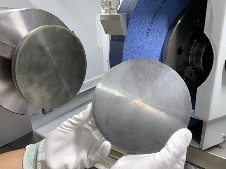
The team analysed the inefficiencies of previous SiC ingot processing methods. The findings were incorporated into the development of an automated all-in-one five-axis machine that can process all currently relevant specifications and diameters of SiC ingots. With automated loading and unloading, the machine can reduce the processing time for an ingot/boule to a puck from more than 24 hours using conventional methods to two to three hours, according to Kellenberger.
In addition to the substrate and the grinding machine, grinding tools play a decisive role in wafer processing. Carmine Sileno, product manager for the semi-conductor sector at
Meister Abrasives, said: “We see semi-conductors as a rapidly growing market.” The company, based in Andelfingen, Switzerland, together with its German sister company Alfons Schmeier, Helmbrechts, specialises in the development and manufacture of superabrasive grinding tools for high-precision grinding applications.
Atomic force microscopy Meister Abrasives offers solutions for the various steps in the semiconductor manufacturing chain, from raw crystal to finished chip, which customers in wafer or chip production can use on existing equipment. The diamond grinding tools developed for the surface of the wafers ensure surface qualities in the range of Ra5 angstrom (1A = 0.0001µm). Mr Sileno says, for comparison — a human hair has a diameter of 40-80µm. Quality assurance for such high surface qualities is only possible using white light interferometry or atomic force microscopy (AFM). He brings wafers to
GrindingHub as an illustration, the surfaces of which can be examined under a microscope.
Mr Sileno emphasised: “Even surfaces with homogeneous nanotopography are extremely important for chip manufacturers.” With its ultra-fine technology, the Swiss company is also pursuing another goal: “We want to grind as finely as possible in order to shorten subsequent process steps or, ideally, eliminate them altogether.” This applies above all to time-consuming and costly lapping and polishing processes.
Wafers are usually ground first and then polished to achieve the required high surface quality. The slurries used for polishing are mixtures of fine solid particles and a liquid. This polishing agent is expensive. The grinding expert continued: “The longer a polishing process usually takes and the larger the wafer area, the more interesting it becomes to minimise the polishing process as much as possible or to remove it from the process altogether.”
The biggest challenge in machining the hard wafer surfaces was to develop the right bond for the sub-micron diamond grain (<1µm). This is precisely where Mr Sileno sees the strength of Meister Abrasives: the ability to customise the abrasive coating structure for each application in detail. The customer saves valuable time thanks to shortened or even superfluous polishing processes, reduces costs, requires less infrastructure, and increases throughput.
The European Union has set itself the goal of significantly increasing its market share in semi-conductor production from the current 9 to 10% in the coming years. The grinding experts definitely see opportunities for their companies in larger volumes. Mr Sileno concluded: “Given the strong dominance of a few suppliers on the global market, we are preferred partners as a customer-specific supplier.”